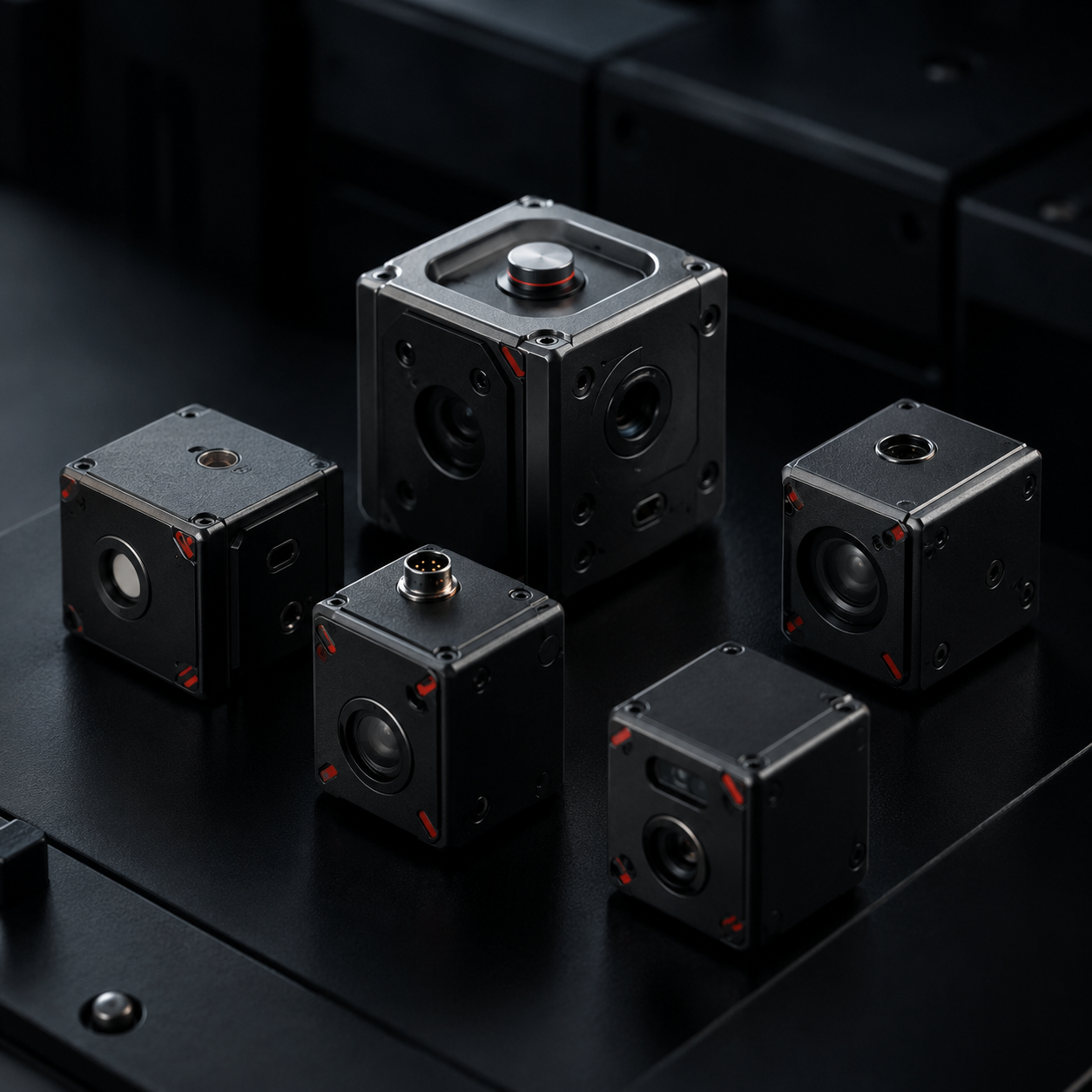
MEMS Design & Fabrication
Body-silicon processing, surface micromachining and wafer bonding for compact sensing structures.
Technology / 01
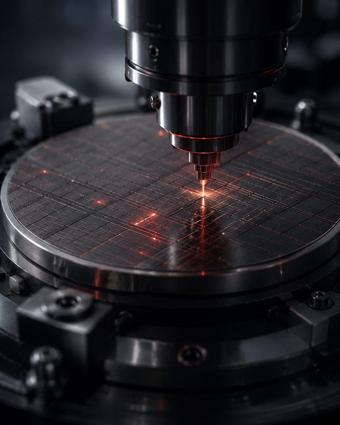
MEMS design, wafer-level packaging and atomic-scale material removal create the stable physical foundation required by precision sensing.
Core Capabilities
Engineering capabilities translated from the company technology framework into a clear deployable stack.
Body-silicon processing, surface micromachining and wafer bonding for compact sensing structures.
Sub-nanometer removal and ultra-low surface damage for advanced semiconductor and inertial structures.
Reliable compact packaging that improves environmental stability and production consistency.
Application Context
The technology is delivered through calibrated products, software interfaces, validation evidence and engineering support rather than as an isolated claim.
Connected Technology Stack
Engineering Contact / Global